
A zinc die-cast housing may look fully enclosed and still leak electromagnetic energy. At 40 GHz, the free-space wavelength is only about 7.5 mm, so a long cover seam or unstable spring contact can matter more than adding metal thickness. This is why an optical transceiver can pass dimensional inspection but fail radiated-emissions testing. The answer is not simply “use zinc” or “add more nickel.” Effective EMI shielding design for die-cast optical transceiver housings requires a continuous conductive shell, controlled joints, reliable contact pressure, and a test plan that finds leakage before certification.
Quick Answer: What Makes a Die-Cast Housing Shield EMI?

A die-cast optical transceiver housing needs four things to shield reliably:
- A conductive enclosure: Zinc alloy provides a useful metal body, but every opening and joint must be included in the shielding path.
- Controlled cover seams: Overlapping or labyrinth joints are more robust than a direct line-of-sight flat joint.
- Low-impedance contacts: Springs, screws, and mating surfaces need enough contact pressure and conductive coverage throughout the product’s life.
- Production control: Gap variation, warpage, plating coverage, and assembly wear must be measured, not assumed.
NASA’s shielding-effectiveness design guidance notes that joints and apertures often limit the shielding effectiveness of an enclosure. For a small transceiver housing, this means the seam around the cover may be more important than the conductivity of the wall itself.
Where Does EMI Escape From an Optical Transceiver Housing?
The most common leakage paths are mechanical interfaces rather than solid metal.
At 10 GHz, the free-space wavelength is about 30 mm. At 40 GHz, it is about 7.5 mm. The seam does not need to be several millimeters wide to radiate. A narrow but electrically long opening can still couple energy from inside the module to the outside.
Design the Cover Joint as Part of the RF Shield
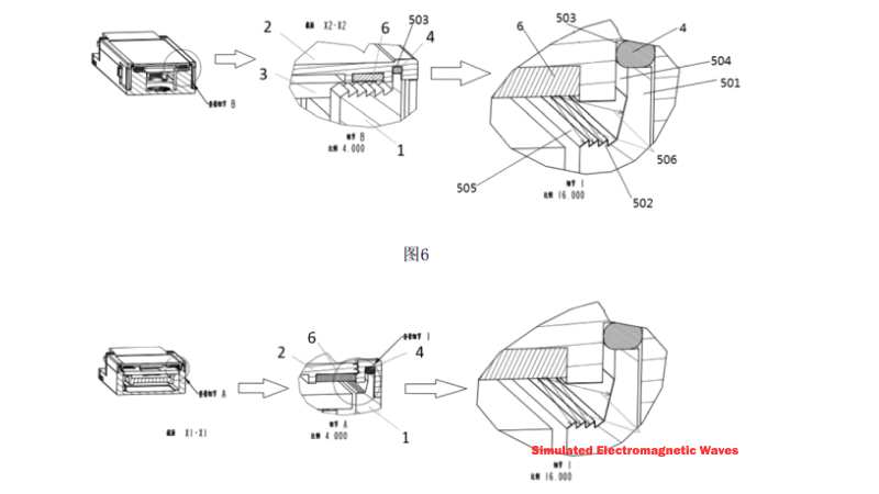
Avoid a Direct Flat Joint When the Frequency Is High
A flat butt joint gives electromagnetic energy a short, direct path through the cover seam. It also depends heavily on perfect flatness and uniform closure force.
A stepped or labyrinth joint forces the leakage path to turn and travel farther. An interlocking tongue and groove also creates overlapping conductive surfaces, making the design less sensitive to one local gap.
The exact overlap, step height, and clearance should not be copied from another housing. They must fit the casting capability, coating thickness, assembly force, and target frequency range.
Control the Entire Seam, Not One Drawing Dimension
A drawing may specify a 0.1 mm joint clearance, but the assembled seam can vary because of casting warpage, parting-line flash, coating buildup, or uneven spring force. Measure the gap around the full perimeter and relate the result to the EMI scan.
NASA’s MSFC grounding and shielding handbook describes unbonded joints and seams as RF apertures and calls for intimate electrical contact to maintain enclosure shielding integrity. In practical terms, one tight measurement point does not compensate for a loose section elsewhere.
Use Grounding Springs to Create Repeatable Contact
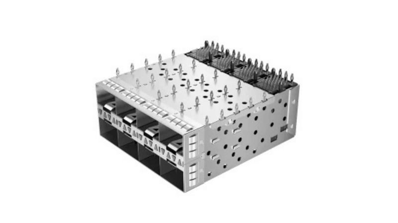
Grounding springs bridge small gaps between the module housing and cage or between mating housing parts. Their effectiveness depends on more than the spring material.
Review these factors together:
- Number and spacing of contact points
- Compressed spring height and working range
- Contact force after repeated insertion and removal
- Flatness and position of the supporting die-cast feature
- Conductivity and wear of the plated contact surface
- Risk of over-compression, permanent set, or assembly damage
A small raised pad beneath a spring can add controlled preload. However, the pad height must be based on the spring’s working range and the housing tolerance stack. Too little preload creates unstable resistance, while too much can damage the spring or make insertion difficult.
For validation, measure the complete contact path using a four-wire method. A two-wire resistance reading includes lead and probe resistance, which can be significant when the target is only a few milliohms. Repeat the measurement after insertion cycles, not only on a new assembly.
Surface Finish Must Keep the Shielding Path Conductive
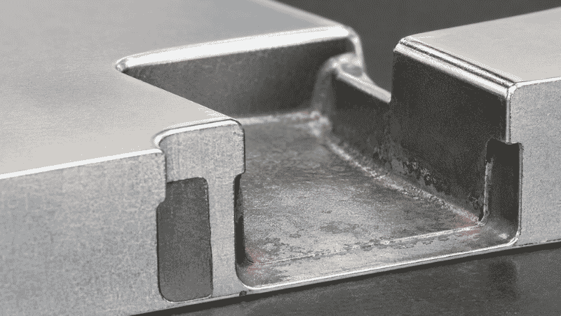
ZAMAK 3 provides the conductive body, but oxides, contamination, paint, and incomplete plating can interrupt the contact surface. A conductive finish should be specified at the seam, spring slot, and other grounding points.
Do not approve a finish from an exterior flat-surface measurement alone. Narrow slots may have different coverage from accessible surfaces. Define coating-thickness measurement points, permitted rack marks, masked areas, and the maximum buildup allowed on clips and locating features.
The process choice is geometry-dependent. Electroless nickel can provide useful deposit distribution on many parts, but it is not automatically better for every zinc housing. Rack plating can also fail inside a recess if the rack position and current distribution are poor. The correct process is the one that demonstrates continuous coverage, adhesion, resistance, and assembly fit on the real part.
For more detail on pretreatment and coating inspection, see Honjenny’s surface-finishing capabilities.
Case Study: Six Radiated-Emission Failures From One Housing Seam
We saw these design issues on a ZAMAK 3 QSFP28 100G upper and lower housing set. The original covers used a flat locating joint with a designed 0.1 mm clearance. Two groups of cage grounding-spring slots were placed along the side, and the bottom of each slot was flat.
The surface finish was electroless nickel-gold, with 2 to 3 µm nickel and 0.05 µm flash gold.
Under the project’s GR-1089-CORE radiated-emissions test from 10 to 40 GHz, six high-frequency points exceeded the limit by 3 to 8 dB. The maximum grounding-path resistance reached 82 mΩ, far above the customer’s requirement of 10 mΩ or less. EMI certification could not continue.
Ericsson’s official GR-1089 page identifies GR-1089 as the generic EMC and electrical-safety criteria for network telecommunications equipment. The 10 to 40 GHz range and 10 mΩ target reported here were the requirements applied to this specific project, not universal limits for every transceiver housing.
How We Located the Leakage
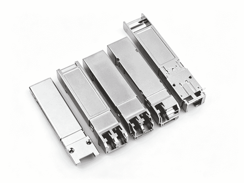
We used a near-field probe to scan around the assembled housing. The strongest leakage followed the upper-to-lower cover seam and the side spring-contact locations.
This method is useful for fault location because it shows relative hot spots before another full chamber test. A Tektronix EMI troubleshooting guide similarly recommends near-field probes for finding leakage from enclosure seams and openings.
Four-wire measurements then showed that spring-contact resistance rose into the hundreds of milliohms after 20 simulated insertion cycles. CMM inspection found that the seam was not uniform, with maximum gap variation reaching 0.08 mm around the perimeter.
The investigation identified three connected causes:
- The direct flat seam acted as an electrically long leakage path at high frequencies.
- Two spring-contact groups did not provide enough distributed contact, and the flat slot floors provided insufficient preload.
- The original coating process showed incomplete conductive coverage in the narrow spring slots.
What We Changed
The flat joint was replaced by a single-step labyrinth structure. The upper and lower cover features overlapped, removing the direct line-of-sight path and extending the route that leaked energy had to follow.
The number of side spring-slot groups increased from two to four. A 0.05 mm raised contact pad was added to each slot floor to increase spring compression and stabilize contact force.
After trials on the revised geometry, the surface process changed from electroless nickel-gold to rack-plated nickel-gold. Nickel thickness was increased to 3 to 5 µm, and coverage inside the functional slots was verified. This was a project-specific result, not evidence that rack plating is always superior to electroless plating.
Results After the Redesign
Radiated emissions across 10 to 40 GHz remained at least 6 dB below the applicable limits. Comparative shielding performance improved by about 12 dB.
Grounding resistance stabilized between 3 and 6 mΩ. After 100 insertion cycles, resistance variation remained within 20%. The customer passed EMI certification on the first test after the correction, while grounding-related assembly defects fell from 18% to below 0.5%.
The result came from three changes working together. The labyrinth joint reduced seam leakage, the additional preloaded springs lowered contact impedance, and verified plating coverage maintained the conductive path.
A Practical EMI Validation Plan
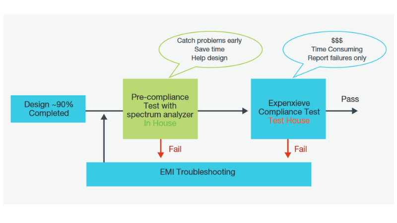
EMI performance should be checked in stages so problems are found before formal certification.
1. Review the Housing and PCB Together
Identify high-speed ICs, clocks, switching power circuits, return-current paths, connectors, and openings. The housing can block energy only after the PCB design controls how that energy reaches the enclosure.
2. Inspect Mechanical and Coating Features
Use CMM data to check joint profile, flatness, spring-slot position, and assembled gaps. Measure coating thickness at grounding points and section difficult recesses during process qualification.
3. Measure Contact Resistance
Define the measurement path and use four-wire testing. Record new-part resistance, then repeat after insertion cycles and environmental testing. The pass limit should come from the customer’s electrical and EMI requirements.
4. Run Near-Field Scans
Scan the cover seam, optical opening, spring contacts, screws, and cable interfaces. Compare the same locations before and after a proposed change. Near-field results locate probable leakage, but they do not replace a calibrated radiated-emissions test.
5. Complete the Required Emissions Test
Use the customer’s specified standard, frequency range, setup, operating mode, and margin. Record which housing revision, coating lot, spring lot, and assembly condition were tested so the result can be reproduced in production.
What to Include in the Drawing and RFQ
Send the die caster more than a 3D model. Include:
- Target EMC standard and frequency range
- Required margin below the emissions limit
- Grounding-resistance limit and measurement path
- Housing alloy and surface-finish stack
- Contact surfaces and coating measurement points
- Cover-joint profile and assembled-gap requirement
- Spring type, quantity, compression range, and cycle target
- Critical flatness, profile, and positional tolerances
- Permitted parting lines, rack marks, and masked areas
- Required CMM, coating, resistance, and EMI reports
Ask for a DFM review before mold release. A small change to the joint, spring floor, or parting line is much less expensive before tooling than after a failed chamber test.
Conclusion
EMI shielding design for a die-cast optical transceiver housing is mainly a problem of continuity. The zinc wall provides the conductive shell, but seams, openings, springs, plating, and production variation decide whether that shell remains electrically closed.
Start with an overlapping joint, distribute reliable contacts around leakage-prone areas, specify conductive finish at the real contact points, and validate performance after repeated assembly. Use near-field scanning and resistance measurements to find problems early, then confirm the complete module with the required radiated-emissions test.
Review Your Housing Before the Next EMI Test
Honjenny provides zinc and aluminum die casting, mold development, CNC machining, and surface finishing for optical transceiver housings. Send us your drawings, EMI requirements, grounding-spring specifications, and critical contact areas for a DFM review of the housing joints, tolerances, and conductive finish. Get a Quote for your optical transceiver housing project.